 EMPC23
The 24th European Microelectronics & Packaging Conference
11-14 September 2023 –
Wellcome Genome Campus, Hinxton
(near Cambridge), UK

Keynote Speaker
Interconnecting Chiplets
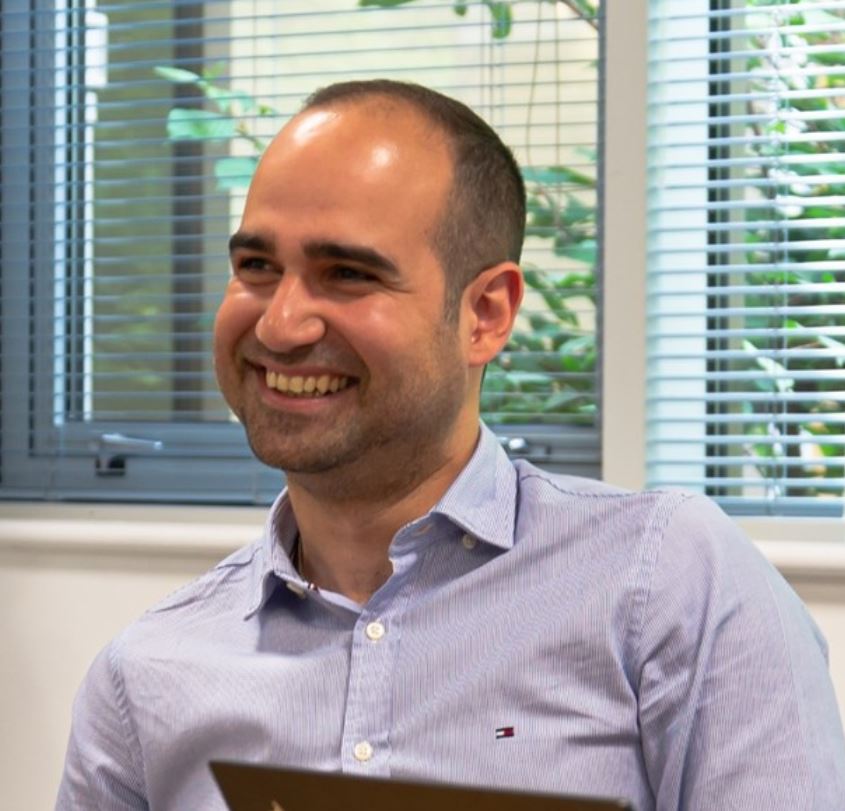
Chris Scanlan, Senior Vice President Technology, BESI Switzerland
Chris Scanlan is Senior Vice President Technology at Besi Switzerland where he is leading advanced technology road map development and technical promotion. Prior to joining Besi he was Vice President of Worldwide Applications Engineering at JCET Group where he was responsible for business development, technical program management and product design. From 2009 to 2019 he was SVP of Product Development at Deca Technologies. Chris was primarily responsible for the development of Deca’s portfolio of intellectual property and technology relating to advanced wafer-level manufacturing methods. Chris worked at Amkor Technology for 10 years where he held leadership positions including VPs of Global R&D, Advanced Products and System in Package business units. Chris started his career at Motorola Semiconductor covering manufacturing of high power IGBT modules and transfer of fcCSP technology from R&D to production. He has 70 issued US patents related to semiconductor packaging. He earned his Master of Science degree in Materials Engineering from the University of Wisconsin-Milwaukee.
Abstract:
The semiconductor industry is undergoing a shift from traditional transistor scaling to heterogeneous integration (HI) using chiplets. While SoC is becoming infeasible for some applications due to the limitations of Moore’s Law, chiplets provide a way to continue system-level scaling through More than Moore. However, chiplet systems can be complex and require a hierarchy of different interconnect types in the same package.
The most advanced interconnect technology for chiplets is hybrid bonding, which connects chips directly with Cu-Cu bonds. Die-to-wafer hybrid bonding has already been in volume production since 2022 for high-performance computing (HPC) applications. However, complete HI systems require other advanced wafer-level assembly processes as well, including TCB, fan-out and bridge die attach, wafer-level flip-chip, and wafer moulding. In the near future, photonic chiplets will be introduced, and together these interconnect methods can form a hierarchy of interconnect in complex chiplet systems.
In this speech we will explore the opportunities and challenges of chiplet integration for continued system-level scaling. We will discuss the different interconnect technologies used in chiplet systems and the advancements in assembly equipment that enable these high density interconnects. We will also examine the importance of collaboration and standardization in the chiplet ecosystem and how they can enable the rapid development of new products and business models.

Advanced Packaging - Challenges that are driving new package innovation & ecosystem needs
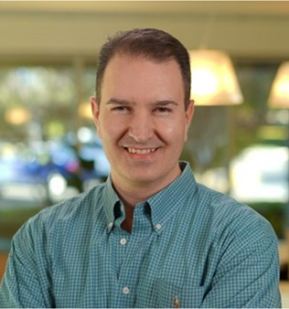
Mark Gerber, Sr. Director Engineering and Technical Marketing, ASE Group
Mark is Sr. Director of Engineering and Marketing at ASE (US) Inc., He manages a team that supports customer activities around the world focused on all market segments with package multiple platform focus areas including Flip Chip, Copper Pillar, Advanced RDL and SiP Packaging Technologies. Mark has +20 years of semiconductor packaging experience working for Advanced Semiconductor Engineering-ASE, Texas Instruments, Motorola and Dallas Semiconductor in various areas of design, manufacturing, and assembly with an emphasis on the development of new technologies and processes. Mark has served as general chair for multiple conferences, led multiple committees for IMAPS and IEEE and is currently serving on the IMAPS executive committee as a director. Mark was awarded the IMAPS Fellow title in 2018. He holds a bachelor’s degree in mechanical engineering from Texas A&M University, has written +20 papers and holds 38 semiconductor packaging patents.
Abstract:
Advanced silicon node challenges, and the drive within industry to find new ways of offering the highest level of performance, are driving many new ways to extend advanced packaging. Many analysts defined advanced packaging as packaging that uses a higher density of interconnect, outside of the traditional wire-bond. This category opens a broad spectrum of packaging solutions that include, Flip Chip, Fan Out Wafer Level Packaging, Hybrid Packaging, System in Package, 2.5D/3D and many sub-categories. As yield enhancement and performance improvements are driving design considerations, such as heterogeneous and homogenous integration, it is becoming more complex to navigate this plethora of new options and to understand the key trade-offs in selecting the right package solution. Challenges including power delivery signal integrity, multi-physics impacts, IP block interface standards, chiplet manufacturing considerations, warpage and many others are driving the ecosystem to change to meet these new and evolving needs. The traditional 2D mindset for silicon integration in packaging is rapidly changing and a 3D or vertical mindset is becoming a key driver for HPC, AI and is extending into mobile products. In this plenary talk, I will discuss these challenges and also talk about some of the solutions as well as needs from the ecosystem to help enable this new era.
Wide Bandgap Devices and Multi-dimensional Architectures in the New Era of Power Electronics
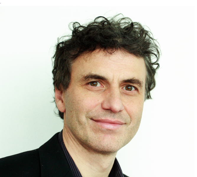
Professor Florin Udrea, Cambridge GaN Devices
Professor Florin Udrea is a professor in semiconductor engineering and head of the High Voltage Microelectronics and Sensors Laboratory at University of Cambridge. He is currently leading a research group in power semiconductor devices and solid-state sensors that has won an international reputation during the last 25 years. Prof. Udrea has published over 500 papers in journals and international conferences and holds over 200 patents in power semiconductor devices and sensors. Prof. Florin Udrea founded five companies, including Cambridge GaN Devices in high voltage GaN technology. For his ‘outstanding personal contribution to British Engineering’ he has been awarded the Silver Medal from the Royal Academy of Engineering. In 2015 Prof. Florin Udrea was elected a Fellow of Royal Academy of Engineering. In 2018 Prof. Udrea has been awarded several major prizes, including the Mullard medal from the Royal Society. In 2020 he received the Ohmi award as a co-author of the ISPSD paper on Silicon Carbide FInFETs. In 2021 he was awarded the academic entrepreneur of the year in UK by Business Weekly.
Abstract:
The power devices field has seen tremendous changes in the last decade. Most of the innovation in the field comes from the emergence of Wide Bandgap semiconductors – and in particular those based on Gallium Nitride and Silicon Carbide. Extensive research is also carried out in single crystal Diamond, Gallium Oxide and Aluminium Nitride materials. The market of power devices has reached ~$50M with exponential growth in wide bandgap materials reaching CAGRs in excess of 50% in the next 3-5 years. This talk will cover an exciting range of wide bandgap (WBG) and ultra wide bandgap (UWBG) semiconductor technologies and materials for power devices. The talk will also address the new multi-dimensional architectures to further increase efficiency of power semiconductor devices.
The challenges of integrating graphene into existing packages
Dr. Ali Murad, Test & Packaging Engineer. Paragraf
Dr. Ali Murad is a Test and Packaging Engineer at Paragraf Ltd., specializing in nanotechnology and semiconductor packaging. With a distinguished background in the field and experience at Intel Corporation and Nexperia Ltd., Dr. Murad brings extensive industry knowledge and expertise. As a sought-after keynote speaker, he shares valuable insights on the latest advancements and trends in nanotechnology and semiconductor packaging.
Abstract:
Graphene has been one of the most exciting materials in recent years for a wide variety of industries ranging from electronics, energy, medicine, sensors, and many more. It has been referred to as a wonder material due to its incredible mechanical strength, lightness, flexibility, optical transparency, and impressive semiconductor properties (of both electricity and heat). Paragraf is the first company in the world to mass produce graphene-based electronic devices using standard semiconductor manufacturing processes, has been at the forefront of this effort. However, there are industrywide challenges related to graphene which Paragraf continues to overcome. Some of the challenges are, getting high-quality uniform contamination-free graphene, managing device integration to graphene, integrating graphene devices to industry standard packaging etc. This talk will focus on discussing these challenges, including how Paragraf is producing high-volume graphene based devices for industry applications. This talk will also focus on the latest development of Paragraf’s technology and how Paragraf is using its technology to solve real-world problems like heat detection in EV batteries, brushless motors, and many more. In summary, this talk is aiming to provide an overview of the challenges of integrating graphene into packages and the role Paragraf is playing in advancing the use of graphene in industrial applications.
Reinventing Electronics for a Sustainable World
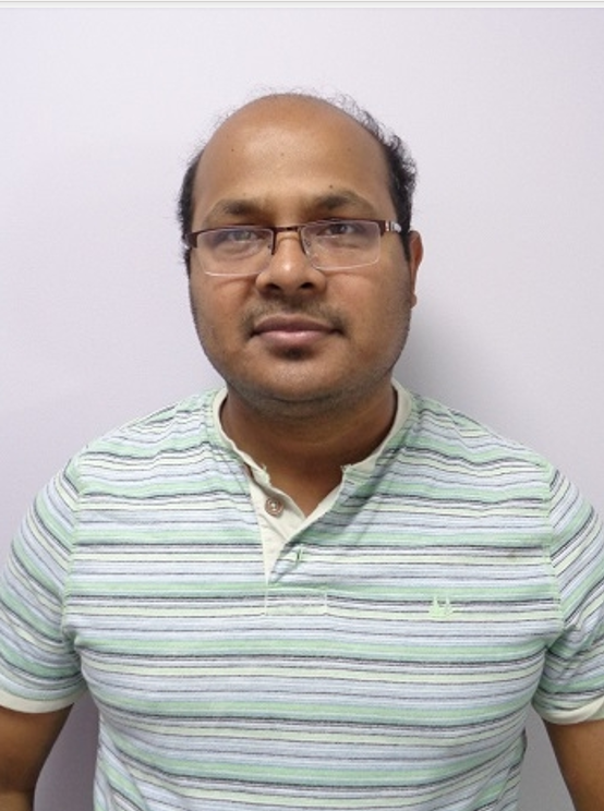
Dr Feras Alkhalil, Principal Scientist and Director of R&D, Pragmatic Semiconductor
Dr Feras Alkhalil is the Director of R&D at Pragmatic Semiconductor. Feras has been leading the Research and Development activities at Pragmatic since 2015, responsible for early-stage technology development. Feras has an Electronics Engineering background and received an MSc and Ph.D. from the University of Southampton in Microelectronics System Design and Solid-State Quantum Electronics, respectively. Feras taught Semiconductor Physics at the University of Southampton in Malaysia 2013-2015, holds a visiting fellowship with Durham University since 2017, and has more than 10 patents and is published in over 18 international journals.
Abstract:
Tackling challenges associated with the climate crisis, sustainability of food supplies and healthcare inequalities require innovative sustainable approaches. Pragmatic Semiconductor is a world leader in the design, development and manufacture of ultra-low-cost Flexible Integrated Circuits (FlexICs). Pragmatic’s FlexICs technology is unique in allowing designers to access extremely agile design cycles, coupled with a low cost and low environmental footprint distributed manufacturing model, this enables sustainable democratised innovation. In this session, we will present Pragmatic’s innovative FlexIC Foundry™, offering novel form-factor integrated circuits, that can be used to create ubiquitous low-cost smart systems. We will also present novel emerging technologies, that we are currently developing, that will enable designers to create even more innovative designs with Pragmatic’s FlexIC Foundry.
